Sn51dp Datasheet -
The physical implementation of the SN51DP is governed by the thermal and mechanical data within the datasheet. The "Thermal Resistance" (RθJA or RθJC) quantifies the component's ability to dissipate heat into the environment. If the SN51DP is a power device, this section dictates the necessity and size of external heatsinks. Furthermore, the package dimensions and pin configurations (often found in the mechanical drawings) are essential for PCB (Printed Circuit Board) layout, ensuring the footprint matches the design software and assembly equipment.
The layout of the SN51DP relies on its 10-pin interface to regulate voltage boost circuits and monitor over-voltage or over-current anomalies. The reference layout maps out as follows: Pin Number Functional Description VIN Main input voltage power supply link. 2 DIM Digital or analog PWM dimming control input line. 3 OVP Over-Voltage Protection sensor node. 4 GND System common ground connection pin. 5 CS Current Sense input; tracks external MOSFET current. 6 ISET
Need more specific parameters or a schematic diagram? Visit professional electronics forums like EEVblog or Badcaps.net, where experienced technicians often share original SN51DP datasheet scans and application notes. sn51dp datasheet
If you suspect the chip is defective, follow these steps:
Yes, due to its BJT design, efficiency is lower (70-80%). A heat sink is mandatory above 500mA. Consider a modern alternative (e.g., LM2596) for new designs. The physical implementation of the SN51DP is governed
For repair technicians, adhering to manufacturer safety standards is essential. When troubleshooting power management ICs, it is recommended to use proper diagnostic tools and refer to the full service manual for the specific television model. For complex repairs involving high-voltage components like backlight drivers, consulting with a licensed electronics professional ensures the device remains compliant with safety regulations.
: Ensure the MSOP10 package has adequate copper pour around the ground pins, as standalone modulators can generate heat during high-frequency switching. 2 DIM Digital or analog PWM dimming control input line
The manufactured by ON-BRIG. It functions as a specialized standalone pulse width modulation (PWM) LED driver. It is widely deployed in liquid crystal display (LCD) applications, specifically managing LED TV backlight driver assemblies. Common hardware environments using this chip include mainboards like the TP.S506.PB801 and TP.MS3463S.PB801 , found inside Arielli, Crown, Felix, and Thomson television sets. Core Specifications and Operating Parameters
Always verify Pin 5 reference voltage and Pin 9 divider network before replacing the IC.
Warning: Bypassing safety mechanisms should strictly be limited to quick testing environments. Running a driver board continuously with disabled OVP can permanently damage the boost circuit or cause thermal runaway on the PCB. Cross-Referencing and Pin-to-Pin Equivalents
Download
Portable EXE (272 KB)
Portable ZIP (244 KB)
Installation Package EXE (863 KB)
Installation Package ZIP (773 KB)
Version: 5.0
Release: March 26, 2020
System Requirements:
Microsoft Windows 11/10/8.1/8/7/Vista/XP
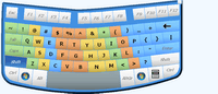
Virtual Keyboard (English)
Virtuelle Tastatur (Deutsch)
Teclado Virtual (Español)
Tastiera Virtuale (Italiano)
Clavier Virtuel (Française)
Teclado Virtual (Português)
Virtueel Toetsenbord (Nederlandse)
Виртуальная клавиатура (Русский)
Sponsor
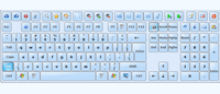
Hot Virtual Keyboard packs a number of advanced features to make on-screen typing faster, easier, and more accurate. Fully customizable look and behavior.
Free Virtual Keyboard Online Help
Free Virtual Keyboard Blog
What's New in Version 5.0
License Agreement
Privacy & Cookies
Contact
Virtual Keyboard | Alarm Clock | Clipboard Manager | On-Screen Keyboard